- 您现在的位置:买卖IC网 > Sheet目录3881 > PIC18F4539T-E/ML (Microchip Technology)IC PIC MCU FLASH 12KX16 44QFN
PIC18FXX39
DS30485A-page 36
Preliminary
2002 Microchip Technology Inc.
4.3
Fast Register Stack
For PIC18FXX39 devices, a “fast interrupt return”
option is available for high priority interrupts. A single
level Fast Register Stack is provided for the STATUS,
WREG and BSR registers; it is not readable or writable.
When the processor vectors for an interrupt, the stack
is loaded with the current value of the corresponding
register. If the FAST RETURN instruction is used to
return from the interrupt, the values in the registers are
then loaded back into the working registers.
4.4
PCL, PCLATH and PCLATU
The program counter (PC) specifies the address of the
instruction to fetch for execution. The PC is 21-bits
wide. The low byte is called the PCL register. This reg-
ister is readable and writable. The high byte is called
the PCH register. This register contains the PC<15:8>
bits and is not directly readable or writable. Updates to
the PCH register may be performed through the
PCLATH register. The upper byte is called PCU. This
register contains the PC<20:16> bits and is not directly
readable or writable. Updates to the PCU register may
be performed through the PCLATU register.
The PC addresses bytes in the program memory. To
prevent the PC from becoming misaligned with word
instructions, the LSB of PCL is fixed to a value of ‘0’.
The PC increments by 2 to address sequential
instructions in the program memory.
The CALL,
RCALL,
GOTO
and program branch
instructions write to the program counter directly. For
these instructions, the contents of PCLATH and
PCLATU are not transferred to the program counter.
The contents of PCLATH and PCLATU will be trans-
ferred to the program counter by an operation that
writes PCL. Similarly, the upper two bytes of the pro-
gram counter will be transferred to PCLATH and
PCLATU by an operation that reads PCL. This is useful
for computed offsets to the PC (see Section 4.8.1).
4.5
Clocking Scheme/Instruction
Cycle
The clock input (from OSC1) is internally divided by
four to generate four non-overlapping quadrature
clocks, namely Q1, Q2, Q3 and Q4. Internally, the pro-
gram counter (PC) is incremented every Q1, the
instruction is fetched from the program memory and
latched into the instruction register in Q4. The instruc-
tion is decoded and executed during the following Q1
through Q4. The clocks and instruction execution flow
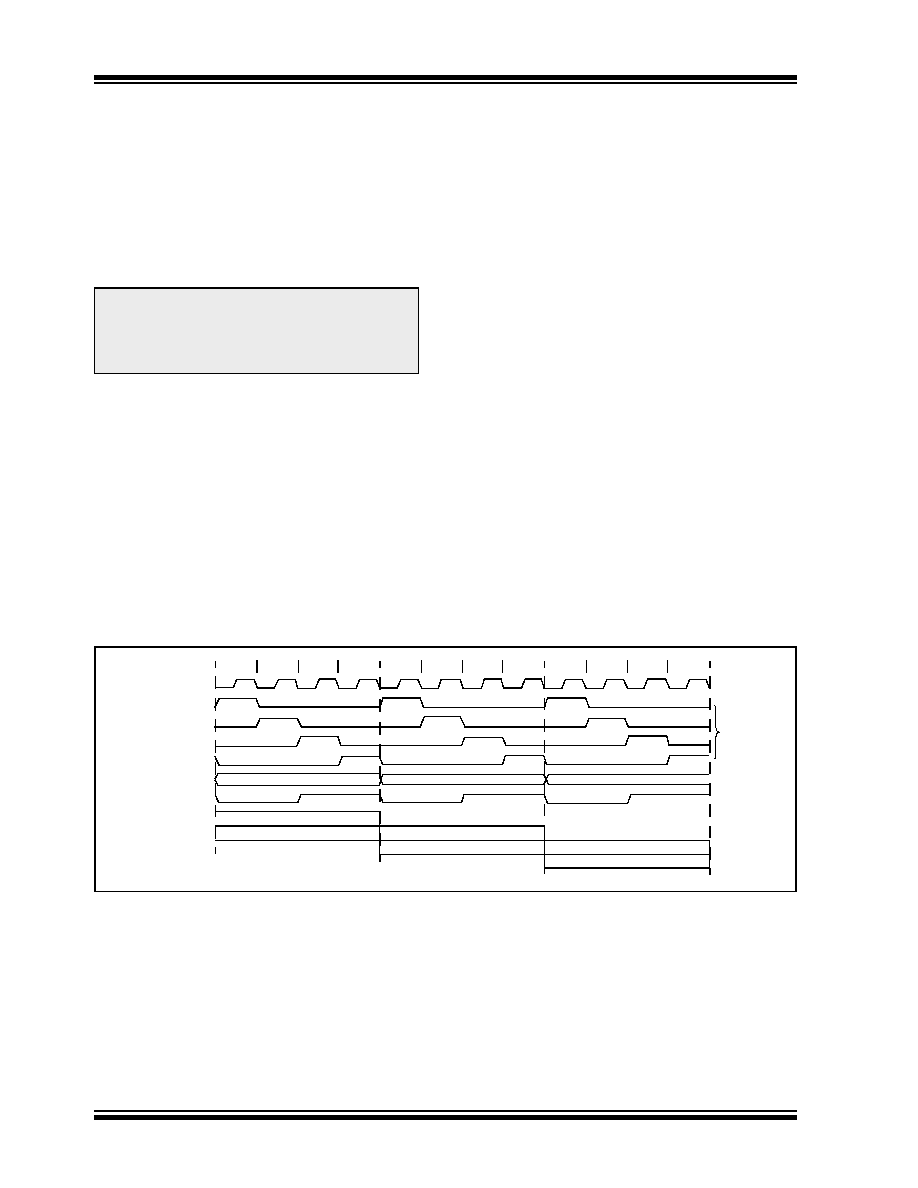
are shown in Figure 4-3.
FIGURE 4-3:
CLOCK/INSTRUCTION CYCLE
Note:
The fast interrupt return for PIC18FXX39
devices is reserved for use by the ProMPT
kernel and the Timer2 match interrupt. It is
not available to the user for any other
interrupts or returns from subroutines.
Q1
Q2
Q3
Q4
Q1
Q2
Q3
Q4
Q1
Q2
Q3
Q4
OSC1
Q1
Q2
Q3
Q4
PC
OSC2/CLKO
(RC mode)
PC
PC+2
PC+4
Fetch INST (PC)
Execute INST (PC-2)
Fetch INST (PC+2)
Execute INST (PC)
Fetch INST (PC+4)
Execute INST (PC+2)
Internal
Phase
Clock
发布紧急采购,3分钟左右您将得到回复。
相关PDF资料
PIC18LF8680T-I/PT
IC PIC MCU FLASH 32KX16 80TQFP
PIC16F1936-I/SO
IC PIC MCU FLASH 512KX14 28-SOIC
PIC18F24K20-I/SO
IC PIC MCU FLASH 8KX16 28SOIC
PIC18LF8585T-I/PT
IC PIC MCU FLASH 24KX16 80TQFP
XF2J-3024-11
CONN FPC 30POS 0.5MM SMT
PIC18LF6525T-I/PT
IC PIC MCU FLASH 24KX16 64TQFP
PIC18LF8621T-I/PT
IC PIC MCU FLASH 32KX16 80TQFP
PIC18F8620T-E/PT
IC PIC MCU FLASH 32KX16 80TQFP
相关代理商/技术参数
PIC18F4539T-E/PT
功能描述:8位微控制器 -MCU 24KB 1408 RAM 32 I/O RoHS:否 制造商:Silicon Labs 核心:8051 处理器系列:C8051F39x 数据总线宽度:8 bit 最大时钟频率:50 MHz 程序存储器大小:16 KB 数据 RAM 大小:1 KB 片上 ADC:Yes 工作电源电压:1.8 V to 3.6 V 工作温度范围:- 40 C to + 105 C 封装 / 箱体:QFN-20 安装风格:SMD/SMT
PIC18F4539T-I/ML
功能描述:8位微控制器 -MCU 24KB 1408 RAM 32 I/O RoHS:否 制造商:Silicon Labs 核心:8051 处理器系列:C8051F39x 数据总线宽度:8 bit 最大时钟频率:50 MHz 程序存储器大小:16 KB 数据 RAM 大小:1 KB 片上 ADC:Yes 工作电源电压:1.8 V to 3.6 V 工作温度范围:- 40 C to + 105 C 封装 / 箱体:QFN-20 安装风格:SMD/SMT
PIC18F4539T-I/PT
功能描述:8位微控制器 -MCU 24KB 1408 RAM 32 I/O RoHS:否 制造商:Silicon Labs 核心:8051 处理器系列:C8051F39x 数据总线宽度:8 bit 最大时钟频率:50 MHz 程序存储器大小:16 KB 数据 RAM 大小:1 KB 片上 ADC:Yes 工作电源电压:1.8 V to 3.6 V 工作温度范围:- 40 C to + 105 C 封装 / 箱体:QFN-20 安装风格:SMD/SMT
PIC18F4550EPT
制造商:Microchip Technology Inc 功能描述:
PIC18F4550-I/ML
功能描述:8位微控制器 -MCU 32kBF 2048RM FSUSB2 RoHS:否 制造商:Silicon Labs 核心:8051 处理器系列:C8051F39x 数据总线宽度:8 bit 最大时钟频率:50 MHz 程序存储器大小:16 KB 数据 RAM 大小:1 KB 片上 ADC:Yes 工作电源电压:1.8 V to 3.6 V 工作温度范围:- 40 C to + 105 C 封装 / 箱体:QFN-20 安装风格:SMD/SMT
PIC18F4550-I/P
功能描述:8位微控制器 -MCU 32kBF 2048RM FSUSB2 RoHS:否 制造商:Silicon Labs 核心:8051 处理器系列:C8051F39x 数据总线宽度:8 bit 最大时钟频率:50 MHz 程序存储器大小:16 KB 数据 RAM 大小:1 KB 片上 ADC:Yes 工作电源电压:1.8 V to 3.6 V 工作温度范围:- 40 C to + 105 C 封装 / 箱体:QFN-20 安装风格:SMD/SMT
PIC18F4550-I/PT
功能描述:8位微控制器 -MCU 32kBF 2048RM FSUSB2 RoHS:否 制造商:Silicon Labs 核心:8051 处理器系列:C8051F39x 数据总线宽度:8 bit 最大时钟频率:50 MHz 程序存储器大小:16 KB 数据 RAM 大小:1 KB 片上 ADC:Yes 工作电源电压:1.8 V to 3.6 V 工作温度范围:- 40 C to + 105 C 封装 / 箱体:QFN-20 安装风格:SMD/SMT
PIC18F4550T-I/ML
功能描述:8位微控制器 -MCU 32kBF 2048RM FSUSB2 RoHS:否 制造商:Silicon Labs 核心:8051 处理器系列:C8051F39x 数据总线宽度:8 bit 最大时钟频率:50 MHz 程序存储器大小:16 KB 数据 RAM 大小:1 KB 片上 ADC:Yes 工作电源电压:1.8 V to 3.6 V 工作温度范围:- 40 C to + 105 C 封装 / 箱体:QFN-20 安装风格:SMD/SMT